Most solid elements in Nature form crystal structures where atoms are arranged in regular lattices. The atoms consist of the heavy and positively charged nucleus surrounded by their electrons and depending on the binding and interactions exhibited by the outermost electrons of the atoms, their collective behaviour determines the diverse phases found in crystalline materials: metallic, semiconducting, insulating, magnetic or superconducting. When electrons are delocalized and free to move through the lattice, the properties are accurately described by so-called Bloch theory. The success of this theory is linked to the overwhelming success of modern semiconductor device technology.
However, in a wide class of materials including many magnets, insulators, and high-temperature superconductors, the electrons are tightly bound to their nucleus and the Bloch theory fails. Instead, the so-called Hubbard model in-principle captures the interactions among the localized electrons. The problem is, however, that the quantum nature of the electrons makes it impossible to solve the model or simulate the solution even the strongest supercomputers. Using electrons confined in semiconductors, researcher have instead tried to design quantum experiments that effectively simulate the Hubbard model. Until now, however, these experiments have failed because of the microscopic disorder inherent to conventional semiconductor electronics.
In this project, we take a new approach to such experiments by growing ultra-pure crystal lattices. The hypothesis is that the microscopic disorder can be eliminated by using position-controlled crystal growth instead of mechanically shaping existing crystals into the relevant geometries. This would enable us to perform quantum simulations of the Hubbard model to guide future developments of new materials such as high-temperature superconductors which could revolutionize technology.

Work during phase 1
For this project, we are developing new methods to use semiconductor process technology to direct crystal growth to specific positions on a surface with nanoscale precision; selective area growth. In the project's first phase, we developed the recipes to increase the control over crystal growth to the scale of less than 100 nanometers. This involves understanding new aspects of crystal growth that dominate when growth selectivity is patterned on the same length scales as the atomic diffusion lengths governing the crystal growth. This gives rise to new proximity effects, both a challenge and a tool for engineering the crystal on the nanoscale.
Gaining statistical significance
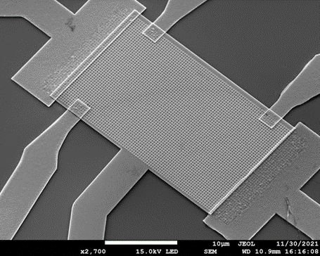
A central hypothesis is that bottom-up nanocrystals may feature more reproducible electrical properties than those realized by conventional top-down processing. To acquire statistical properties of nanoscale electrical devices at ultra-low temperatures, we developed an on-chip multiplexer device that allows semiautomatic addressing of thousands of individual devices in a single cool-down. The multiplexer devices comprise nearly ten thousand interconnected selective area grown nanowires and are the first example of scalable integrated circuits based on bottom-up nanostructures. The multiplexers operate successfully because of the high yield of our nanostructures. Multiplexers will be an essential tool for the project and for future mesoscopic devices based on selective area growth. In the first iteration, we employed the multiplexers to benchmark the statistical properties of selective area grown nanowire transistors, quantum dots, and to statistically correlate crystal growth parameters with their electrical performance.

With the developed methods for patterning, we can now achieve selective area growth (SAG) in dense patterns at a scale beyond the state of the art for growth using semiconductor molecular beam epitaxy. With these dense patterns we also enter growth regimes that are beyond the state of the art; we continue to deepen our understanding as analysis progresses. The SAG-based multiplexers are the first example of integrated cryogenic electronics using bottom-up nanostructures and constitute a milestone for the field. Quantifying the statistical distributions of electrical parameters has not previously been possible - the yield and statistical device-to-device variability are promising for the use of SAG in quantum simulation devices.
In the coming phase of the project, we will continue to improve the ultra-dense selective area crystal growth using the multiplexer platform for statistically quantifying the progress. Here a focus will be to move from single elements to larger coupled systems and networks. This adds a new dimension to the complexity of both devices and crystal growth
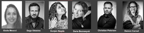
As of November 1st the following researchers are involved in TURNSTONE
- PhD student Christian Emanuel Noes Petersen
- PhD student Giulia Meucci
- Post-doc Dr. Daria Beznasiuk
- Development engineer Dr. Damon Carrad
- PI Prof. Thomas Sand Jespersen
Previous contributors
- PhD Dags Olsteins
- PhD Gunjan Nagda